

Introduction
PCB layout online is the process of designing printed circuit boards using cloud-based or web-supported software tools. These tools allow students, engineers, and professionals to design PCBs without installing heavy applications. Online PCB layout platforms are widely used for learning, prototyping, and professional electronics projects because they save time, reduce cost, and improve design efficiency.
Step 1 Define PCB Requirements
The first step in PCB layout online is defining the project requirements. This includes deciding the board size, number of layers, type of components, voltage levels, and current ratings. Clear requirements help designers plan the layout properly and avoid design changes at later stages.
Step 2 Create the Schematic
After finalizing the requirements, the schematic diagram is created. The schematic shows how electronic components are connected electrically. Online PCB layout tools provide built-in component libraries, making it easy to place components and draw connections accurately. A correct schematic is the foundation of a reliable PCB layout.
Step 3 Assign Component Footprints
Each component used in the schematic must be assigned a physical footprint. Footprints define the pad size, shape, and pin spacing on the PCB. Online PCB layout software offers standard footprint libraries that help ensure correct component mounting and smooth manufacturing.
Step 4 Place Components on the PCB
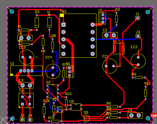
Component placement is a critical step in PCB layout online. Components should be placed logically based on circuit function, signal flow, and power distribution. Sensitive components should be kept away from high-power sections to reduce noise and interference. Proper placement simplifies routing and improves circuit performance.
Step 5 Route PCB Traces
Routing connects the component pins using copper tracks. Online PCB layout tools support both manual and auto-routing options. Designers must follow routing rules such as trace width, spacing, and clearance. Power and ground traces should be wider to safely carry higher current.
Step 6 Add Ground Plane and Power Routing
Adding a ground plane helps reduce electrical noise and improves signal stability. Online PCB layout platforms make it easy to create ground planes and manage power routing. Proper placement of decoupling capacitors near ICs is also important for stable circuit operation.
Step 7 Perform Design Rule Check
Design Rule Check is used to identify errors such as short circuits, spacing violations, and unconnected pins. Online PCB layout tools automatically check the design based on manufacturing standards. Running DRC ensures the PCB is error-free before fabrication.
Step 8 Generate Manufacturing Files
The final step in PCB layout online is generating manufacturing files such as Gerber files, drill files, and Bill of Materials. These files are required by PCB manufacturers to produce the board accurately and efficiently.