
Introduction
Circuit analysis is an important step in PCB reverse engineering. It helps engineers understand how an electronic circuit works by studying the connections between components on a Printed Circuit Board (PCB). During this process, engineers analyze the circuit structure, identify electronic components, and trace the electrical connections that form the complete circuit.
In many cases, the original schematic diagram of a PCB may not be available. Circuit analysis allows engineers to examine the PCB and determine how signals flow through the circuit. By studying the copper traces and component connections, engineers can understand the function of each part of the circuit and recreate the circuit diagram using PCB design tools such as Altium Designer.
Circuit analysis is widely used in electronics repair, product research, and hardware design improvement. It is also very useful for engineering students who want to learn how real electronic circuits are designed and implemented.
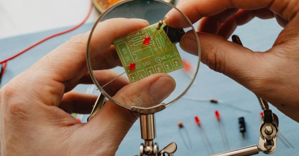
Visual Inspection of the PCB
The first step in circuit analysis is carefully inspecting the printed circuit board. Engineers observe the PCB to identify major components such as integrated circuits, resistors, capacitors, and connectors. They also study the board layout and note how components are arranged on the PCB.
Visual inspection provides an overview of the circuit and helps engineers understand the general structure of the design.
Identifying Electronic Components
The next step is identifying all the electronic components present on the PCB. Each component usually has a printed code or marking that indicates its value or part number.
Engineers use these markings to determine the type of component and its specifications. For example, resistors have resistance values, capacitors have capacitance ratings, and integrated circuits have part numbers that can be referenced in their datasheets.
Correctly identifying components is essential because it helps engineers understand the function of each part of the circuit.
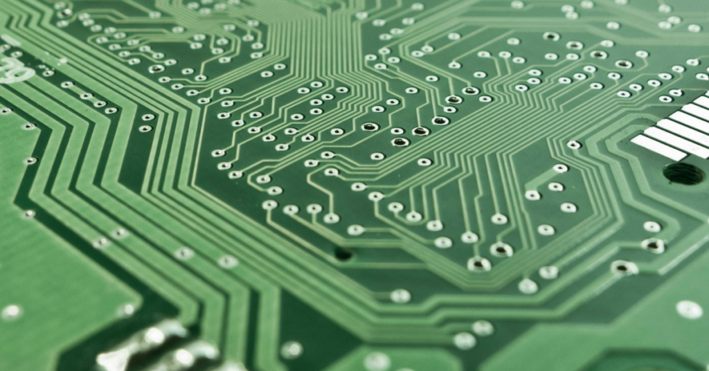
Tracing Copper Connections
After identifying the components, engineers trace the copper tracks on the PCB to determine how the components are connected. These copper traces act as electrical pathways that carry signals and power between different parts of the circuit.
Tools such as a multimeter can be used to check electrical continuity between points on the PCB. This helps verify the connections and ensures accurate circuit analysis.
Understanding Signal Flow
Once the connections are traced, engineers analyze how signals travel through the circuit. They study how power enters the board, how signals are processed by integrated circuits, and how the output signals are generated.
Understanding signal flow helps engineers determine the purpose of the circuit and how each section of the board functions.
Creating a Circuit Diagram
The final step in circuit analysis is creating a schematic diagram that represents the circuit. Engineers draw the circuit using PCB design software, placing component symbols and connecting them based on the traced PCB connections.
This schematic diagram provides a clear representation of the circuit and helps engineers study, modify, or reproduce the design.
Conclusion
Circuit analysis is a crucial step in PCB reverse engineering because it helps engineers understand the design and functionality of electronic circuits. By carefully inspecting the PCB, identifying components, tracing connections, and recreating the schematic diagram, engineers can fully analyze and rebuild the circuit. This process is valuable for electronics repair, product analysis, and learning practical PCB design techniques.