
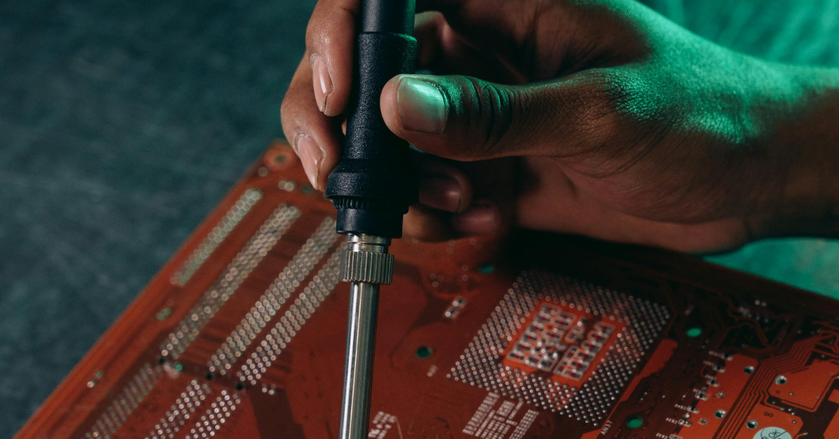
PCB board fabrication is a precise process that transforms circuit designs into functional electronic boards essential for modern devices. This guide outlines key steps in points for clarity, optimized for searches like “PCB fabrication process steps” and “how to fabricate PCB boards.”
Design Preparation
- Engineers create schematics and layouts using software like Eagle or KiCad, defining traces, pads, and layers.
- Gerber files are generated, including drill files and solder masks, ensuring manufacturer compatibility.
- Design Rule Checks (DRC) verify spacing, width, and clearances to avoid errors during production.
Material Selection
- Copper-clad laminates (FR4 common) form the base, with copper foil thickness typically 1-2 oz per square foot.
- Prepreg sheets insulate multi-layer boards, chosen based on glass transition temperature for reliability.
- Substrate options like Rogers suit high-frequency needs, while standard FR4 handles general applications.
Inner Layer Processing
- Photoresist coats copper layers, exposed to UV light via artwork films to define circuit patterns.
- Etching removes excess copper, followed by stripping resist and oxide treatment for bonding.
- Automated Optical Inspection (AOI) scans for defects like shorts or opens early in the flow.
Lamination
- Inner layers stack with prepreg and copper foil, aligned via pins for precision registration.
- Hydraulic presses apply 375°F heat and 275-400 psi pressure, melting epoxy to fuse layers.
- Cooling cures the stack, creating a solid multi-layer core ready for outer processing.
Drilling and Plating
- CNC machines drill vias and holes per files, with depths controlled to ±0.1mm accuracy.
- Electroless copper deposits a thin conductive layer (20 microns minimum) on hole walls.
- Electroplating thickens copper to 25-35 microns, enabling electrical connectivity across layers.
Outer Layer Imaging
- Photoresist applies again, imaging outer circuits matching inner alignment targets.
- Etching defines traces, tin plating protects copper from final etch, then stripped.
- Solder mask prints green (or custom) epoxy over non-pad areas for insulation and protection.
Finishing and Testing
- Silkscreen adds labels and markings; surface finishes like ENIG or HASL apply for solderability.
- Electrical testing (flying probe or bed-of-nails) verifies continuity and isolates faults.
- Final visual checks, routing, and packaging prepare boards for assembly.