
Printed Circuit Board (PCB) design is a core skill in electronics engineering. Every electronic device, from small consumer gadgets to advanced industrial systems, depends on a properly designed PCB. Understanding PCB design basics helps beginners build reliable, efficient, and manufacturable electronic circuits. This article explains PCB design basics in a simple, step-by-step manner suitable for students and professionals.
What Is PCB Design?
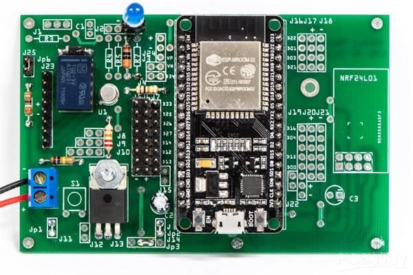
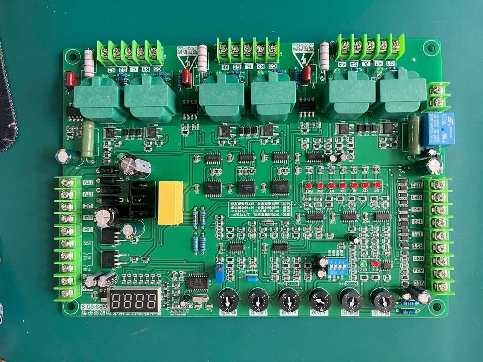
PCB design is the process of converting an electronic circuit into a physical board layout using copper tracks, pads, and components. A PCB provides mechanical support and electrical connections for electronic components. It replaces complex wiring and ensures compact, organized, and reliable circuit construction. Learning PCB design basics is essential for anyone entering the electronics field.
Importance of PCB Design Basics
Strong PCB design fundamentals help reduce circuit errors, improve signal quality, and ensure smooth manufacturing. Proper PCB design increases product reliability, minimizes noise, and reduces production costs. Without basic PCB knowledge, even a good circuit idea may fail during fabrication or testing.
Understanding Circuit Requirements
The first step in PCB design basics is understanding the circuit requirements. This includes identifying the circuit function, power supply voltage, current capacity, number of components, and board size. Clear requirements help avoid design mistakes and save time during later stages of PCB development.
Creating the Schematic Diagram
The schematic diagram represents the logical connection of components. In this step, electronic components such as resistors, capacitors, diodes, and integrated circuits are placed and connected according to the circuit design. A correct and verified schematic forms the foundation of a successful PCB layout.
Selecting Components and Footprints
Component selection plays a key role in PCB design basics. Choose components based on electrical ratings, package type, and availability. After selecting components, assign proper PCB footprints. Footprints define pad size, spacing, and component shape on the PCB. Accurate footprints ensure correct soldering and assembly.
Component Placement on PCB Layout
Component placement determines the performance and reliability of the PCB. Related components should be placed close together, and power components should be separated from sensitive signal components. Logical placement improves signal flow, reduces interference, and simplifies routing.
Routing PCB Tracks
Routing is the process of connecting component pads using copper tracks. Track width must be selected based on current requirements. Avoid sharp angles and unnecessary vias. Proper routing is essential to maintain signal integrity and reduce electrical noise.
Grounding and Power Distribution
Good grounding and power planning are critical parts of PCB design basics. Using a solid ground plane helps reduce noise and improves circuit stability. Power lines should be routed carefully to avoid voltage drops and interference.
Design Rule Check and Verification
Design Rule Check verifies the PCB layout against manufacturing rules. It detects errors such as short circuits, spacing violations, and unconnected pins. Performing this check ensures the PCB is ready for fabrication and reduces costly errors.
Generating Manufacturing Files
After final verification, manufacturing files such as Gerber files, drill files, and bill of materials are generated. These files are required by PCB manufacturers to fabricate and assemble the board accurately.
Conclusion
PCB design basics are the foundation of electronic hardware development. By following a structured, step-by-step approach, beginners can design efficient and reliable printed circuit boards. Strong fundamentals in PCB design lead to better performance, fewer errors, and professional-quality electronic products.