
Printed Circuit Board (PCB) fabrication and assembly are critical processes in modern electronics manufacturing. From consumer gadgets to industrial equipment, PCBs form the backbone of electronic systems. Understanding the step-by-step process of PCB fabrication and assembly helps designers, engineers, and manufacturers ensure quality, reliability, and performance. This article explains the complete workflow in a simple and structured manner.
Step 1: PCB Design and Layout Preparation
The PCB fabrication process begins with circuit design. Engineers use PCB design software to create schematics and convert them into board layouts. This layout defines copper traces, pad sizes, component placement, and board dimensions. Design Rule Checks (DRC) are performed to eliminate errors before fabrication. Once finalized, the design files such as Gerber, drill, and BOM files are generated.
Step 2: Material Selection
Choosing the right PCB material is essential for durability and performance. Commonly used substrates include FR-4, aluminum, and flexible materials. The selection depends on factors like operating temperature, electrical requirements, and application type. Copper thickness and board layers are also decided at this stage.
Step 3: PCB Fabrication Process
PCB fabrication involves transforming the design into a physical board.
- Printing the Circuit Pattern: The Gerber file is used to print the circuit pattern onto a copper-clad laminate.
- Etching: Unwanted copper is removed using chemical etching, leaving behind the desired circuit traces.
- Drilling: Holes are drilled for through-hole components and vias.
- Plating: Copper is electroplated inside drilled holes to ensure electrical connectivity between layers.
- Solder Mask Application: A protective solder mask layer is applied to prevent short circuits and oxidation.
- Silkscreen Printing: Component labels, symbols, and markings are printed on the board surface.
After these steps, the fabricated PCB undergoes visual and electrical inspection.
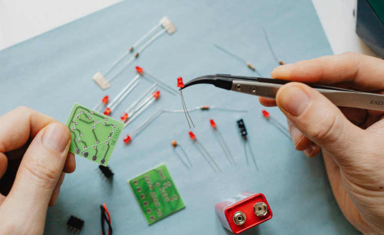
Step 4: PCB Assembly Preparation
PCB assembly begins once the bare board is ready. This stage includes preparing components, solder paste, and assembly machines. The Bill of Materials (BOM) guides the selection and quantity of components. Proper preparation ensures smooth and error-free assembly.
Step 5: Solder Paste Application
Solder paste is applied to the PCB pads using a stencil. This paste acts as both a temporary adhesive and a conductive material during soldering. Accurate paste application is crucial to avoid solder bridges or weak joints.
Step 6: Component Placement
Components are placed onto the PCB using automated pick-and-place machines or manually for low-volume production. Surface Mount Technology (SMT) components are placed with high precision, while Through-Hole Technology (THT) components are inserted later if required.
Step 7: Soldering Process
The soldering process secures components to the PCB.
- Reflow Soldering: Used for SMT components, where the board passes through a reflow oven to melt solder paste.
- Wave Soldering: Commonly used for THT components, where the PCB passes over a wave of molten solder.
This step ensures strong electrical and mechanical connections.
Step 8: Inspection and Testing
Quality inspection is vital in PCB assembly. Techniques such as Automated Optical Inspection (AOI), X-ray inspection, and functional testing are used to detect defects. Electrical testing ensures the PCB operates as intended.
Step 9: Final Cleaning and Packaging
After testing, the assembled PCB is cleaned to remove flux residues and contaminants. Finally, boards are packaged using anti-static materials to prevent damage during transportation.
Conclusion
PCB fabrication and assembly are systematic processes that require precision at every stage. From design and material selection to assembly and testing, each step plays a vital role in ensuring high-quality electronic products. Understanding this step-wise workflow helps manufacturers deliver reliable and efficient PCBs for various applications.