
Introduction
Schematic and PCB recreation is an essential stage in the PCB reverse engineering process. After analyzing the circuit and tracing the connections on a Printed Circuit Board (PCB), engineers recreate the schematic diagram and PCB layout using design software. This step helps engineers fully understand the electronic circuit and reproduce the original board design.
In many cases, the original schematic files or design documents are not available. By recreating the schematic and PCB layout from the physical board, engineers can analyze how the circuit functions and make improvements if necessary. This process is widely used in electronics repair, product analysis, and hardware development.
Modern PCB design software tools, such as Altium Designer, are commonly used to recreate schematic diagrams and PCB layouts accurately. These tools help engineers organize components, draw circuit connections, and design professional PCB layouts.
Collecting PCB Information
The first step in recreating a schematic and PCB is gathering all necessary information from the existing PCB. Engineers examine the board carefully and note details such as component placement, board dimensions, and copper trace connections.
They also identify all electronic components used in the circuit, including resistors, capacitors, diodes, and integrated circuits. Component markings and datasheets are often used to determine the correct component specifications.
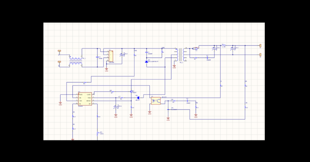
Creating the Schematic Diagram
After collecting the required information, engineers begin recreating the schematic diagram. A schematic diagram represents the electrical connections between components using standard electronic symbols.
Engineers place component symbols in the design software and connect them according to the traced circuit connections. This step converts the physical PCB connections into a clear and organized electrical diagram.
The schematic diagram helps engineers understand the circuit’s logical operation and identify the system’s functional blocks.
Verifying the Circuit Connections
Once the schematic diagram is created, engineers verify that all connections match the original PCB. They compare the schematic diagram with the traced PCB connections to ensure accuracy.
This step is important because incorrect connections may lead to errors in the recreated design. Engineers carefully check power lines, ground connections, and signal paths to confirm that the schematic accurately reflects the original circuit.
Recreating the PCB Layout
After verifying the schematic diagram, engineers begin designing the PCB layout. The PCB layout represents the physical arrangement of components and copper traces on the circuit board.
Engineers place component footprints on the board according to the original PCB placement. They then route copper traces to connect the components while maintaining proper spacing and design rules.
This step ensures that the recreated PCB layout closely matches the original board design.
Final Review and Optimization
The final step in recreating the schematic and PCB is to review the design and make any necessary improvements. Engineers check the layout for any design rule violations, incorrect connections, or missing components.
If needed, modifications can be made to improve the circuit performance, reduce noise, or optimize the PCB layout. After verification, the recreated PCB design can be used for manufacturing or further analysis.
Conclusion
Schematic and PCB recreation is a critical part of PCB reverse engineering, helping engineers transform a physical circuit board into a digital design. By recreating the schematic diagram and PCB layout, engineers can understand the circuit operation, modify the design, and reproduce the PCB when needed. This process plays an important role in electronics repair, product development, and learning practical PCB design techniques.