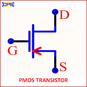
A PMOS Transistor (P-type Metal-Oxide-Semiconductor Field-Effect Transistor) is a type of MOSFET (Metal-Oxide-Semiconductor Field-Effect Transistor) in which the majority charge carriers are holes. It is used as a switch or amplifier in digital and analog circuits and operates in enhancement mode or depletion mode, depending on the application.

Key Features of a PMOS Transistor
- Structure:
- Composed of a P-type channel with two N-type regions (source and drain) and an insulated gate.
- Operation:
- Conducts when the voltage at the gate (VGV_GVG) is lower than the voltage at the source (VSV_SVS).
- A negative voltage is required between the gate and the source to turn it ON.
- Symbol:
- Represented with an arrow on the source pointing outward, indicating hole flow (conventional current direction).
Working Principle:
- OFF State:
- When the gate voltage (VGV_GVG) is equal to or higher than the source voltage (VSV_SVS), the transistor remains off, as no conductive channel forms.
- ON State:
- When a negative voltage is applied to the gate relative to the source (VG<VSV_G < V_SVG<VS), a conductive channel forms, allowing current to flow from the source to the drain.
Applications of PMOS Transistors:
- Digital Logic Circuits:
- Used in CMOS (Complementary Metal-Oxide-Semiconductor) technology alongside NMOS transistors for efficient logic gates.
- Analog Circuits:
- Utilized in amplifiers, current mirrors, and switching circuits.
- Power Management:
- Found in power distribution circuits where low-resistance P-type paths are required.
Advantages:
- Low power consumption in CMOS configurations.
- High input impedance minimizes power loss.
Disadvantages:
- Slower operation compared to NMOS transistors due to lower mobility of holes.
- Requires a negative gate voltage, making design slightly more complex.
